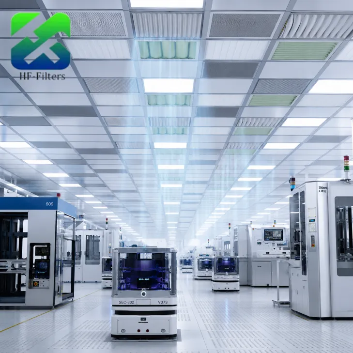
A restaurant kitchen that can cook ten thousand meals an hour is still only as fast as its pass window — the narrow counter where plates leave the kitchen. The semiconductor industry has announced more than $640 billion in fab construction to build kitchens, yet AI supply in 2026 is being rationed at the pass window: advanced packaging.
In the same quarter global chip sales jumped 35.1 percent quarter-over-quarter to $403.3 billion, locking in a path past $1.5 trillion in annual sales, the competitive center of gravity shifted from transistor to package — Nvidia reserved the majority of TSMC’s advanced-packaging capacity, TSMC began bringing its first U.S. packaging fabs to Arizona, and High-NA EUV entered production at Intel while TSMC balked at the tool’s economics. Simultaneously, the U.S.–China chip conflict mutated into a reciprocal tariff-and-minerals regime: Washington cleared H200 shipments subject to a 25 percent levy, and Beijing listed 24 U.S. and EU entities, including American rare-earth miners, on its export-control roster.
THE PASS WINDOW: PACKAGING IS THE NEW LITHOGRAPHY
Mainstream coverage fixates on lithography, but allocation is decided at the back end. CoWoS and 2.5D-interposer capacity — not EUV wafer starts — now rations Blackwell-class supply, and Nvidia’s reservations amount to vertical integration executed through purchase orders. The consequence ripples outward: Broadcom’s custom-silicon roadmaps, AMD’s MI-series and hyperscaler in-house accelerators all compete for the same interposer slots, and sovereign-AI programs are discovering that national compute strategies are hostage to a packaging queue. TSMC’s Arizona packaging fabs — the first advanced-packaging capacity on U.S. soil — mean the reshoring story that actually matters is back-end, not front-end, and the industry’s margin pool is migrating toward interconnect IP, substrates and hybrid bonding.
THE 1986 PRECEDENT: TRADE WARS REDRAW MAPS, MODELS DECIDE WINNERS
The closest analog is the 1986 U.S.–Japan Semiconductor Trade Arrangement and the SEMATECH consortium that followed. The arrangement’s price floors protected U.S. memory makers briefly, raised costs for downstream OEMs and sheltered incumbents from competitive discipline — they still exited DRAM within a decade. The era’s winners were entrants running new models: Samsung’s counter-cyclical capex and TSMC’s pure-play foundry, founded in 1987 as trade friction reorganized the map. The lesson for 2026 is uncomfortable: export controls and tariffs redraw geography, but business-model shifts decide winners. The H200 levy is a price floor with the same side effects, and today’s model shift is the chiplet-and-packaging stack; whoever owns interconnect standards and the pass window takes the decade.
A $1.5 TRILLION BOOM WITH A NARROW BASE
The headline numbers are real: the Semiconductor Industry Association’s August 6 release put Q2 sales at $403.3 billion, up 35.1 percent from Q1, with June up 123.6 percent year-over-year and 2026 annual sales projected to top $1.5 trillion. But an SIA–Deloitte study quantifies how narrow the base is: semiconductors account for 95 percent of an AI server rack’s value, and chips deployed in AI data centers could generate over $1.2 trillion in annual revenue by 2028. Concentration like that means the boom is effectively one end-market: HBM and DDR5 inflation is already pushing smartphone, PC and automotive BOMs higher while mature-node utilization lags. The CHIPS Act timeline compounds the mismatch — Intel’s 18A is in high-volume production in Arizona, but Ohio slips to 2030 and most subsidized capacity reaches volume in 2028–2030, after this cycle’s peak, with the advanced-manufacturing tax credit expiring in December 2026.
CAPITAL DISCIPLINE IS NOT A CHOKEPOINT
The scarcity narrative deserves its own rebuttal. TSMC’s public position — that High-NA EUV tools “can cost up to $400 million each” and “remain too expensive for use at this stage” — is capital discipline, not technological surrender; at its A16 node, multi-patterning on low-NA tools still wins on cost per transistor. The same logic applies to packaging: panel-level packaging, Intel’s EMIB and UCIe-based chiplet interchange are credible 2027–28 alternatives to CoWoS rationing, and HBM4 capacity additions already carry oversupply risk in analyst models. Scarcity at the pass window is a capex cycle, not a law of physics; treating it as permanent would misprice roughly $100 billion of incoming capacity.
THE SECOND CHOKEPOINT: MINERALS AS STRATEGY
The most underreported axis is materials. In June and July 2026, Beijing added ten U.S. entities — including rare-earth miners MP Materials and USA Rare Earth — and 14 EU firms to its export-control roster, extending gallium, germanium and rare-earth restrictions that S&P Global warns will keep supply bottlenecks in place through 2026. Every EUV tool, HBM stack and EV motor sits downstream of those elements: polishing slurries, phosphors, permanent magnets, precursors. The chokepoint narrative that used to run one way — Dutch lithography, Taiwanese front-end — now runs both ways, and procurement is shifting from just-in-time to sovereign stockpiling. Local electronics manufacturers will feel it not as headlines but as lead times: thirty-week quotes on magnets and optics becoming routine.
MANAGED ESCALATION IS NOT DECOUPLING
The doom reading cuts the other way and is equally one-sided. The cooling of U.S. controls and the H200 tariff framework are not incoherence but monetized dependence: earlier control rounds slowed China’s advanced-node yields, the levy converts gray-market demand into revenue and telemetry, and the allied control coalition with Japan and the Netherlands has held. China’s minerals leverage is real but depletable — non-Chinese separation and magnet capacity is scaling in Texas, Australia and Estonia. What 2026 shows is managed escalation: two powers taxing each other’s dependencies while goods keep flowing. Decoupling is the slogan; tariff-and-license statecraft is the operating reality.
POSITIONING FOR THE 2027 CONTRACT CYCLE
- Manufacturers and SMBs: lock long-term agreements for mature-node and memory components now for 2027; audit rare-earth exposure (magnets, phosphors, GaAs/GaN); qualify second sources; assume HBM-driven memory inflation in every BOM.
- Investors: distinguish allocation-driven revenue — packaging, HBM, interconnect, substrates — from broad AI-chip beta; watch TSMC’s High-NA stance as the sector’s capex-discipline indicator.
- Workers and citizens: fab-construction trades and tool-install technicians are the tightest labor market in America; community-college semiconductor programs are placing near 100 percent; consumers should expect device price pressure into 2027.
- Municipalities: water and power guarantees, not tax abatements, are winning fab spillover investment; the bottleneck is utilities.
FEBRUARY 2027: THE ALLOCATION ECONOMY MATURES
Six months out: the first High-NA logic chips ship from Intel as ASML delivers its EXE:5200, while TSMC holds for A14 and its cost model stays unchanged; H200 China volumes under the levy normalize, and Beijing licensing delays trigger the first formal G7 stockpile response; SIA monthly data crosses the $1.5 trillion annualized run-rate, memory inflation produces OEM margin warnings, and the first HBM4 oversupply notes circulate; Congress answers the lapsed manufacturing credit with a stopgap; and the December construction deadline generates a wave of milestone announcements while Ohio remains a 2030 story. The pass window, not the kitchen, will decide who gets served.
Primary sources: SIA market-data releases, Aug. 6 and June 5, 2026; SIA–Deloitte AI server rack study, June 1, 2026; TrendForce/TSMC statements on High-NA EUV economics; S&P Global critical-minerals outlook, 2026; CHIPS Act fab-status tracking, mid-2026.